Brand: PValley
Model: DL-378L6
Country of Origin: Taiwan
Manufacturer: Bangladesh
Features:
- Suitable for combination logic, sequential logic and microprocessor circuits design and experiments
- Ideal tool for learning the basics of digital logic circuits Comprehensive power, signal supply and testing devices for convenient experiments.
- Experiments are expandable and flexible with universal breadboard
- Capable of processing TTL, CMOS, NMOS, PMOS and ECL circuits
- All supply units are equipped with overload protection for safety purpose
- All modules equipped with 8-bit DIP switch for fault simulations
- Individual keeping cases for all modules for easy storing and carrying
- All signal generators have independent and simultaneous TTL and CMOS level output terminal.
General Specification:
Body Material:
Printed Front Side Sheet
Sheet Type: Digital
Country of origin: China
Feature:
- Sheet number 26
- Storage Printed temperature 300°c
- Color White/Silver
Hard Round support board or Plastic Sheet
Sheet Type: Digital
Country of origin: Pakistan
Feature:
- Sheet thickness 10mm
- Two-Part Combination(Transparent/white)
- UV Printout
Panel Box
Brand: Madhav Enterprise
Country of origin: Indian
Features:
- Shape: Rectangular
- Surface Finish: Smooth
- High-quality raw material
Best structure
Brand: Altech
Country of origin: Bangladesh
Feature:
- Sheet thickness 5mm
- Sheet (Silver/white)
- Square Shape
Power Monitoring
Brand: UNI-T
Country of origin: China
Feature:
- Self-operating voltage 12V
- Self-Consumption Current 20mA
- Power Nature
Use Connector
Brand: ZHT
Country of origin: China
Feature:
- Banana Female Connector Diameter 4.5mm
- Banana Male Connector Diameter 4.5mm
Working area:
- Working area: 40 * 25 inch
Technical Specifications:
- Main Unit
- Dual DC Power Supply
(1) Voltage range: +5V/1.5A, -5V/0.3A, ±12V/0.3A
(2) With output overload protection
- Adjustable DC Power Supply
(1) Voltage range: +1.5V ~ +15V
(2) Max. current output: 0.5A
(3) With output overload protection
- Standard Frequency
(1) Frequency: 1MHz, 60Hz, 1Hz
(2) Accuracy: ±0.01% (1MHz)
(3) Fan out: 10 TTL load
- Clock Signal Generator
(1) Frequency: 1Hz ~ 1MHz (6 ranges)
a.1Hz ~ 10Hz
b.10Hz ~ 100Hz
c.100Hz ~ 1KHz
d.1KHz ~ 10KHz
e. 10KHz ~ 100KHz
f. 100KHz ~ 1MHz
(2) Fan out: 10 TTL load
- Data Switch
(1) 8-bit DIP switch x 2, 16-bit TTL level output
(2) Toggle switch x 4, each with Debounce circuit
(3) Fan out: 10 TTL load - Pulser Switch
(1) 2 sets of independent control output
(2) Each set with Q, Q’ output, pulse width > 5ms
(3) Each set of switches with Debounce circuit
(4) Fan out: 10 TTL load - Line Signal Generator
(1) Frequency: 50Hz/60Hz
(2) Output voltage: 6Vrms
(3) With overload protection - Thumbwheel Switch: 2-digit, BCD code output and common point input
- Logic Indicator
(1) 16 sets of independent LEDS indicate high /low logic state
(2) Input Impedance: ≥ 100K ohms - Digital Displays
(1) 4 sets of independent 7-segment LED display
(2) With BCD, 7-segment decoder/driver and DP input
(3) Input with 8-4-2-1 code - Logic Probe
(1) TTL and CMOS level
(2) 5mm LED displays
(3) “Lo” and “Hi” LED display low/high logic state respectively - Speaker: 8 ohms, 0.25W speaker with driver circuit
- Breadboard Modules: 1680 tie-point breadboard on top panel can be easily put into and taken off.
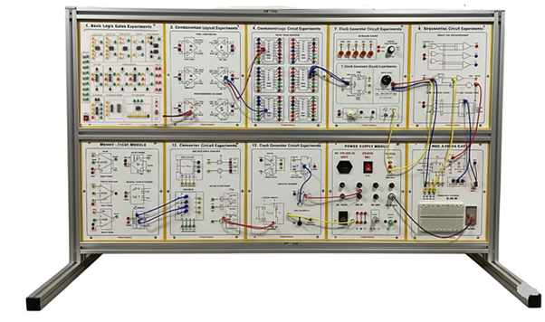
Experiment Modules
- All 13 modules are equipped with an 8-bit DIP switch for fault simulation. Users learn how to solve various. Problems by setting the DIP switch to different positions.
- Solutions for all fault test are listed in the experiment manual for user’s reference.
- 2mm plugs and sockets are used throughout the main unit and all modules.
- Comprehensive experiment manual and instructor’s manual.
- Module dimension: (255 x 165 x 30) mm.
- Connection plugs are used on the modules to prevent accidental damages
- Individual keeping case for each module.
List of Modules
- Basic Logic Gates Experiments
2. Combinational Logic Circuit Experiments (1)
3. Combinational Logic Circuit Experiments (2)
4. Combinational Logic Circuit Experiments (3)
5. Combinational Logic Circuit Experiments (4)
6. Combinational Logic Circuit Experiments (5)
7. Clock Generator Circuit Experiments
8. Sequential Logic Circuit Experiments (1)
9. Sequential Logic Circuit Experiments (2)
10. Memory Circuit Experiments (1)
11. Memory Circuit Experiments (2)
12. Converter Circuit Experiments (1)
13. Converter Circuit Experiments (2)
List of Experiments
- Basic Logic Gates Experiments
(1) Introduction to logic gates and switches
(2) Logic gates circuits
- Diode Logic (DL) circuit
b. Resistor-Transistor Logic (RTL) circuit
c. Diode-Transistor Logic (DTL) circuit
d. Transistor-Transistor Logic (TTL) circuit
e. CMOS logic circuit
(3) Threshold voltage measurement
- TTL threshold voltage measurement
b. CMOS threshold voltage measurement
(4) Voltage/current measurement
- TTL I/O voltage/current measurement
b. CMOS voltage/current measurement
(5) Basic logic gate transmission delay measurement
- TTL gate delay time measurement
b. CMOS gate delay time measurement
(6) Measurement of basic logic gates characteristics
- AND gate characteristics measurement
b. OR gate characteristics measurement
c. INVERTER gate characteristics measurement
d. NAND gate characteristics measurement
e. NOR gate characteristics measurement
f. XOR gate characteristics measurement
(7) Interface between logic gates
- TTL to CMOS interface
- CMOS to TTL interface
- Combinational Logic Circuits Experiments
- (1) NOR gate circuits
- (2) NAND gate circuit
- (3) XOR gate circuit
- Constructing XOR gate with NAND gate
- Constructing XOR gate with basic gate
- (4) AND-OR-INVERT (AOI) gate circuit
- (5) Comparator circuit
- Comparator constructed with basic logic gates
b. Comparator constructed with TTL IC
- (6) Schmitt gate circuit
- (7) Open-collector gate circuits
- High voltage/current circuit
b. Constructing an AND gate with open-collector gate
- (8) Tristate gate circuits
- Truth table measurements
b. Constructing an AND gate with tristate gate
c. Bidirectional transmission circuit
- (9) Half-adder and full-adder circuits
- Constructing HA with basic logic gates
b. Full adder circuit
c. High-speed adder carry generator circuit
d. BCD code adder circuit
- (10) Half-subtractor and full-subtractor circuit
- Subtractor circuit constructed with basic logic gates
b. Full adder and inverter circuit
- (11) Arithmetic Logic Unit (ALU) circuit
- (12) Bit parity generator circuit
- Bit parity generator constructed with XOR gates
b. Bit parity generator IC
- (13) Encoder circuit
- Constructing a 4-to-2 encoder with basic gates
b. Constructing a 10-to-4 encoder with TTL IC
- (14) Decoder circuit
- Constructing a 2-to-4 decoder with basic gates
b. Constructing a 4-to-10 decoder with TTL IC
c. BCD to 7-segment decoder
- (15) Multiplexer circuit
- Constructing a 2-to-1 multiplexer
b. Using multiplexers to create functions
c. Constructing a 8-to-1 multiplexer with TTL IC
- (16) Demultiplexer circuit
- Constructing a 2-output demultiplexer
b. Constructing a 8-output demultiplexer
- (17) Digitally controlled analog multiplexer/demultiplexer circuit
- Analog switch characteristics
b. Bidirectional transmission with CMOS IC analog switches
- Clock Generator Circuit Experiments
(1) Constructing oscillator circuit with basic logic gates
(2) Constructing oscillator circuit with schmitt gate
(3) Voltage controlled oscillator (VCO) circuit
(4) 555 IC oscillator circuit
- 555 oscillator circuit
b. VCO circuit
(5) Monostable multi vibrator circuits
- Low-speed monostable multi vibrator circuits
b. High-speed monostable multi vibrator circuits
c. Constructing monostable multivibrator circuits
d. Constructing non-retrigger able circuit with TTL-IC
e. Constructing retrigger able circuit with TTL-IC
f. Constructing a variable duty cycle oscillator circuit with monostable multi vibrator
- Sequential Logic Circuit Experiments
(1) Flip-flop circuits
- Constructing a R-S flip-flop with a basic logic gate
b. Constructing a D flip-flop with a R-S flip-flop
c. Constructing a J-K flip-flop with a D flip-flop
d. Constructing a J-K flip-flop with a R-S flip-flop
e. Constructing a shift register with a D flip-flop
f. Preset left/right shift register
g. Constructing a noise elimination circuit with R-S flip-flop
- (2) J-K flip-flop circuits
- Asynchronous binary up-counter
b. Asynchronous decade up-counter
c. Asynchronous divide-by-N up-counter
d. Asynchronous binary down-counter
e. Synchronous binary up-counter
f. Synchronous binary up/down counter
g. Preset able synchronous binary up/down counter
h. Preset able synchronous decimal up/down counter
i. Ring counter
j. Johnson’s counter
- Memory Circuit Experiments
(1) Constructing Read Only Memory (ROM) with diodes
(2) Constructing Random Access Memory (RAM) with D flip-flop
(3) 64-bit RAM circuit
(4) Erasable Programmable Read Only Memory (EPROM) circuit
(5) Electronic EPROM (EEPROM) circuit
(6) Constructing dynamic scanning counter with single-chip microprocessor
- Converter Circuit Experiment
(1) Digital/Analog Converter (DAC) circuit
- Unipolar DAC circuit
b. Bipolar DAC circuit
(2) Analog/Digital Converter (ADC) circuit
- 8-bit converter circuit
- 3 1/2-digit converter circuit
Interfacing Software:
- Built-in circuit simulation of experiment modules.
- Fault simulation is allowed.
- Users can flexibly compare the simulation analysis result with hardware signal output.
- Support virtual instrument.
Protection System
- Over-Current Protection
- Short-Circuit Protection
- Over-Voltage Protection
- Earth Leakage / ELCB Protection
- Emergency Stop (E-Stop)
Standard Accessories
- Power Cord
- External Switch Module
- Male to Male Banana Connector
- Experiment Manual and Instructor’s Manual
- Connection Leads and Plugs
- 5 Days In-House Training
Warranty Period: One (1) Year
Reviews
There are no reviews yet.