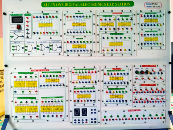
Brand: PValley
Model: DE-2128L
Country of Origin: China
Country of Assemble/Manufacturing: Bangladesh
General Specification:
Body Material:
Printed Front Side Sheet
Sheet Type: Digital
Country of origin: China
Feature:
- Sheet number 26
- Storage Printed temperature 300°c
- Color White/Silver
Hard Plastic Sheet
Sheet Type: Digital
Country of origin: Pakistan
Feature:
- Sheet thickness 10mm
- Two-Part Combination(Transparent/white)
- UV Printout
Power supply
Brand: Biologic Tech
Country of origin: Taiwan
Features:
- 24V/5A SMPS Power Supply
Panel Box
Brand: Madhav Enterprise
Country of origin: Indian
Features:
- Shape: Rectangular
- Surface Finish: Smooth
High quality raw material
Power Monitoring
Brand: UNI-T
Country of origin: China
Feature:
- Self-operating voltage 12V
- Self-Consumption Current 20mA
- Power Nature
Use Connector
Brand: ZHT
Country of origin: China
Feature:
- Banana Female Connector Diameter 2mm
- Banana Male Connector Diameter 2mm
Working area:
Working area: 24*30 inch
Technical Specification:
- Module 01: Logic Gates(Basic & Combinational).
- Main Hardware ICs(74LS08/4081, 74LS32/4071, 74LS04/4069, 74LS00/4011, 74LS02/4001, 74LS86 / 4030, 74LS266 / 4077 )
- Operating Voltage +5V DC (TTL) / +3 to 15 V DC (CMOS)
- Input Logic Levels TTL compatible (0–0.8 V LOW, 2–5 V HIGH)
- Output Logic Levels TTL/CMOS standard
- Power Consumption < 1 W
- Input Current ≤ 1 mA
- Output Drive LED compatible via current-limiting resistor
- Module 02: Assembled Logic Circuits(Half Adder & Full Adder).
- Main Hardware ICs(74LS08,74LS32 & 74LS86)
- Number of Input/Output Lines: 10/4
- Package/Case: PDIP-16
- Propagation Delay Time: 32 ns
- Supply Voltage Range: (2 -6)VDC
- Mounting Style: Through Hole
- Minimum Operating Temperature Range : (- 55 C to + 125)0 C
- Packaging/function/Hight: Tube/Encoder/4.57 mm
- High Level and Low Level Output Current: (- 5.2 to 5.2) mA
- Maximum Clock Frequency: 28 MHz
- Module 03: Assembled Logic Circuits(Encoders and Decoders)
- Main Hardware ICs(74LS147/74LS148, 74LS138/74LS139)
- Operates with a single power supply of +5 volts
- DC with a tolerance of ±5%.
- The input LOW to HIGH voltage level is up to (0.8 to 2V) volts
- The output voltage LOW to HIGH does not exceed (2.0 to 2.4) volts.
- The propagation delay of the gate is approximately 10 nanoseconds.
- The typical power dissipation is around 10 milliwatts.
- The fan-out capability is up to 10 standard TTL loads.
- The operating temperature range is from 0°C to 70°C.
- Module 04: Assembled Logic Circuits (ALU)
- Main Hardware ICs(74LS181)
- Technology Family: LS
- Designed specifically for high speed
- Provides 16 Arithmetic Operations Add, Subtract, Compare, Double, Plus Twelve Other Arithmetic Operations
- Provides all 16 Logic Operations of Two Variables Exclusive OR, Compare, AND, NAND, OR, NOR, Plus Ten other Logic Operations
- Full Lookahead for High Speed Arithmetic Operation on Long Words
- Input Clamp Diodes & ESD protection
- Input Supply Range (4.75 to 5.25)V
- Typical propagation delay: 21nS
- Low power consumption: 32mW
- Operating temperature: 0ºC to 70ºC
- Module 05: Assembled Logic Circuits (Multiplexer & Demultiplexer)
- Main Hardware ICs(74LS151 & 74LS153)
- Technology Family: LS
- Supply voltage: 5.25V
- Frequency at nominal voltage: 35 MHz
- Typical propagation delay: 21nS
- Low power consumption: 30mW
- Channels & Bits : 1/16
- Digital input leakage (Max) (uA): 5
- Operating temperature: 0ºC to 70ºC
- ESD CDM (kV)/HBM (kV): 0.75/2
- Balanced propagation delays
- Designed specifically for high speed
- IOH (Max) to IOL (Max) Range : (-0.8 to16)mA
- Module 06: Assembled Logic Circuits (Registers)
- Main Hardware ICs(74HC595)
- 8-bit serial input
- 8-bit serial or parallel output
- Storage registers with 3-state outputs
- Shift registers with direct clear
- 100 MHz (typical) shift out frequency
- ESD protection:
- HBM JESD22-A114F exceeds 2000 V
- MM JESD22-A115-A exceeds 200 V
- Module 07: Clock Generator Circuit(HA17555)
- Precision timer integrated circuit designed for generating accurate time delays and oscillations
- Wide supply voltage range from (4.5 V to 5) VDC.
- 8‑pin dual in‑line package (DIP‑8), suitable for through‑hole mounting
- Includes trigger and reset pins for flexible timing control.
- Can sink and source currents up to ~200 mA, capable of driving moderate loads directly.
- Output is TTL compatible, suitable for interfacing with standard digital logic circuits.
- Typical timing variation with temperature is around 50 ppm/°C, ensuring reliable operation across normal temperature ranges.
- Available in a standard 8-pin DIP (dual in-line package) for through-hole mounting.
- Module 08: Sequential Logic Circuits (Flip-Flop)
- Main Hardware ICs(74LS73/74LS74/74LS76/74LS112/74LS107)
- Contains two independent D-type flip-flops.
- Triggering: Positive-edge triggered.
- Pins: D (data), CLK (clock), PRE (preset), CLR (clear), Q, Q̅.
- Supply Voltage: +5 V DC (TTL compatible).
- Propagation Delay: ~15 ns.
- Fan-Out: 10 standard TTL loads.
- Module 09: Sequential Logic Circuits (Counter)
- Main Hardware ICs(7490/7493/74192/74193)
- Type: Asynchronous (ripple) decade counter.
- Counting Range: 0–9 (decimal).
- Inputs: Clock, reset (clear).
- Outputs: 4-bit BCD outputs (Q0–Q3).
- Triggering: Negative-edge clock input.
- Supply Voltage: +5 V DC (TTL compatible).
- Propagation Delay: ~22 ns per flip-flop.
- Module 10: Memory Circuits (Random Access Memory)
- Main Hardware ICs(6116A/6264A)
- Type: Static RAM.
- Memory Capacity: 8K words × 8 bits (8192 × 8).
- Inputs: Address lines (A0–A12), Data input (D0–D7), Chip Enable (CE), Write Enable (WE).
- Outputs: Data output (Q0–Q7).
- Supply Voltage: +5 V DC TTL compatible.
- Access Time: ~150–200 ns.
- Package: 28-pin DIP.
- Module 11: Memory Circuits (Read Only Memory)
- Main Hardware ICs(27C16/27C32/27C128/27C512)
- Type: Erasable Programmable ROM (EPROM).
- Memory Capacity: 2K words × 8 bits.
- Access Time: 200 ns typical.
- Inputs: Address lines (A0–A10), Chip Enable (CE), Output Enable (OE).
- Outputs: Data output (Q0–Q7).
- Programming: UV light erasable via quartz window.
- Supply Voltage: +5 V DC TTL compatible.
- Package: 24-pin DIP.
Experiment List for Module(1-11):
- Verification of Basic Logic Gates (AND, OR, NOT, NAND, NOR, XOR, XNOR)
- Implementation of Universal Gates Using NAND and NOR
- Design and Testing of Half Adder Circuit
- Design and Testing of Full Adder Circuit
- Design and Testing of Half Subtractor Circuit
- Design and Testing of Full Subtractor Circuit
- Construction of 4-Bit Binary Adder Using IC 7483
- Design of BCD Adder Circuit
- Implementation of Binary-to-Gray and Gray-to-Binary Code Converter
- Design and Verification of Decimal-to-BCD Encoder Using IC 74147
- Implementation of 8-to-3 Priority Encoder Using IC 74148
- Design and Testing of BCD-to-Decimal Decoder Using IC 7442
- Construction of 3-to-8 Line Decoder Using IC 74138
- Implementation of 4-to-1 Multiplexer Using IC 74153
- Implementation of 8-to-1 Multiplexer Using IC 74151
- Design and Testing of 1-to-4 Demultiplexer Using IC 74155
- Design and Testing of 1-to-8 Demultiplexer Using IC 74138 / 74154
- Design of Parity Generator and Parity Checker
- Construction of 4-Bit Magnitude Comparator Using IC 7485
- Implementation of SR Flip-Flop Using NOR/NAND Gates
- Design and Testing of JK Flip-Flop (Toggle and Memory Operation)
- Implementation of D-Type Flip-Flop and Edge-Triggered Data Storage
- Design and Testing of T-Type Flip-Flop (Toggle Operation)
- Construction of Serial-In Serial-Out (SISO) Shift Register Using IC 74164
- Construction of Serial-In Parallel-Out (SIPO) Shift Register
- Construction of Parallel-In Serial-Out (PISO) Shift Register Using IC 7495
- Construction of Parallel-In Parallel-Out (PIPO) Shift Register
- Design and Testing of Ring Counter Using Flip-Flops
- Design and Testing of Twisted Ring (Johnson) Counter
- Implementation of Asynchronous (Ripple) Counters (Binary and Decade)
- Construction of Synchronous 4-Bit Up Counter Using Flip-Flops
- Construction of Synchronous 4-Bit Down Counter Using Flip-Flops
- Design of Up/Down Counter Using IC 74193 or IC 74192
- Design and Implementation of Mod-n Counter
- Implementation of Monostable Multivibrator Using Flip-Flop / IC 555 / HA17555
- Implementation of Astable Multivibrator Using Flip-Flop / IC 555 / HA17555
- Design of Frequency Divider Using Flip-Flops and Counters
- Design and Testing of Predefined Sequence Generator Using Flip-Flops
- Implementation of Digital Clock Using Counters and Flip-Flops
Warranty -1 year
Accessories:
- Power Cord: 01 Set
- Connecting Wire & Cable
- Complete 5 days Training Included
- User Manual or User Guide
Protection:
Under voltage, Supply over voltage, Drive overload, Short Circuit etc.
Reviews
There are no reviews yet.